

PRODUCT
- 首頁
- /
- 產品介紹
- /
- 先進封裝相關
先進封裝相關
-
iAS大面積曝光機
iAS系列創新整面光刻機,適用於高階顯示器、封裝晶片、先進封裝等領域的Micro-LED大面積曝光、封裝晶片大面積曝光和扇出大晶片曝光。
VIEW MORE

-

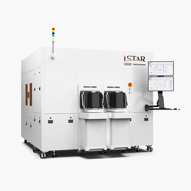
iAB 自動晶圓鍵合設備
iAB系列自動晶圓鍵合設備,能夠實現晶圓與晶圓自動鍵合。 設備採用了一體式設計,無需鍵合夾具,具有鍵合精度高、良率高的優勢。
VIEW MORE
-
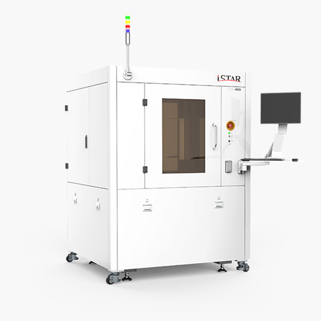
iCB 自動晶片鍵合設備
iCB系列產品為星空科技自主研發的自動晶片鍵合設備,可實現晶片與晶片、晶片與晶圓鍵合。適用於紅外線感測器、MicroLED、Chiplet、真空元件封裝等應用
VIEW MORE
-

SAICAS Interfacial Analysis System
SAICAS 用於透過比較剝離強度來測量油漆和塗料的附著力,以及評估材料的剪切強度。 該儀器還執行對角線切割作為表面分析的預處理。標準樣品尺寸從平板約 20 x 20 毫米到 50 x 50 毫米,最大厚度為 10 毫米。 隨著評估薄膜(例如亞微米和多層薄膜)的可剝離性、黏合性和強度的需求不斷增長,可靠的方法卻很稀缺。 由於材料強度和結構的影響,這些評估具有挑戰性。 然而,表面和界面性質分析儀透過切割方法測量薄膜的黏附力和剪切強度來解決這個問題。
VIEW MORE
-

WSI-300晶圓AOI設備
VIEW MORE
-
NV-F 2D/3D Hybrid Automation System - NV-F2700
最先進的非接觸式 3D 表面輪廓儀。
VIEW MORE
-
NV-F 2D/3D Hybrid Automation System - NV-F3200
最先進的非接觸式 3D 表面輪廓儀。
VIEW MORE


