

PRODUCT
- 首頁
- /
- 產品介紹
- /
- 化合物半導體相關
化合物半導體相關
-
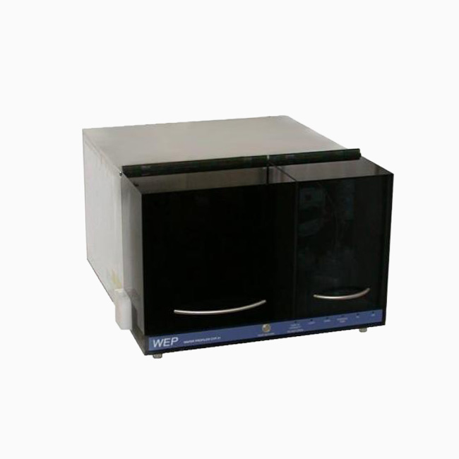
ECV PROFILER CVP21
VIEW MORE

-
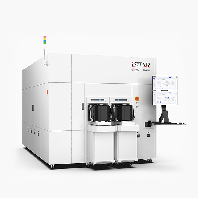
iAS大面積曝光機
iAS系列創新整面光刻機,適用於高階顯示器、封裝晶片、先進封裝等領域的Micro-LED大面積曝光、封裝晶片大面積曝光和扇出大晶片曝光。
VIEW MORE
-
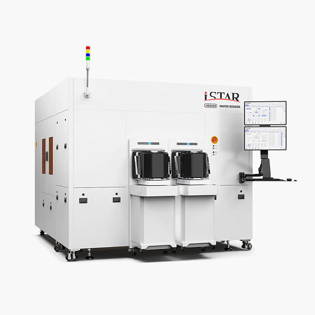
iAB 自動晶圓鍵合設備
iAB系列自動晶圓鍵合設備,能夠實現晶圓與晶圓自動鍵合。 設備採用了一體式設計,無需鍵合夾具,具有鍵合精度高、良率高的優勢。
VIEW MORE
-
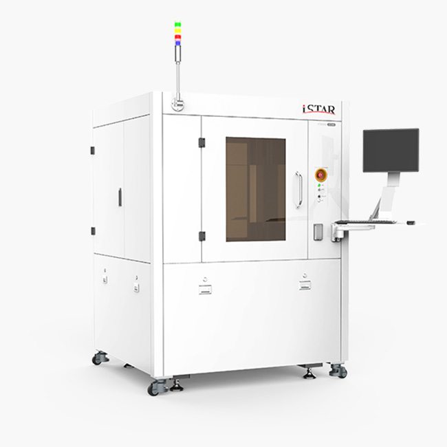
iCB 自動晶片鍵合設備
iCB系列產品為星空科技自主研發的自動晶片鍵合設備,可實現晶片與晶片、晶片與晶圓鍵合。適用於紅外線感測器、MicroLED、Chiplet、真空元件封裝等應用
VIEW MORE
-
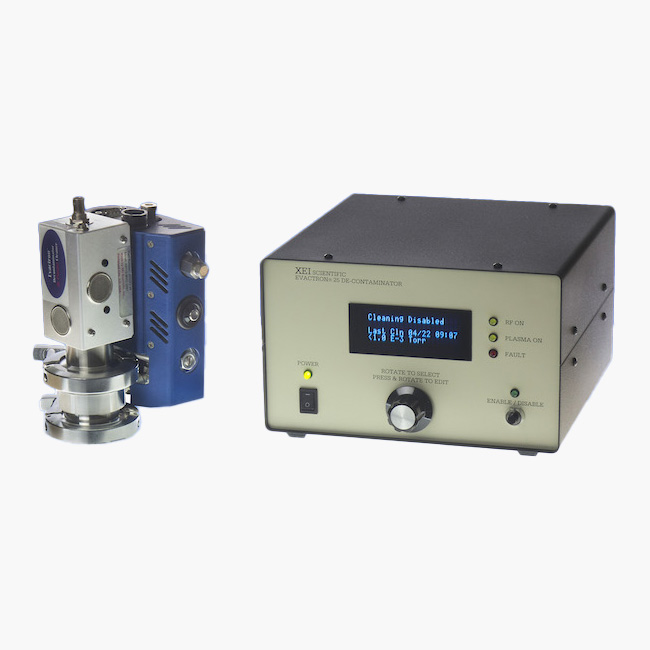
Evactron® Model E25 Plasma De-Contaminators™
Evactron® E25 透過儲存在其內部記憶體中的工廠編程設定簡化了等離子操作,從而減少了對操作員進行大量培訓的需要。 這款緊湊型桌上型控制器具有嵌入式軟體,可調節洩漏閥並透過 MicroPirani™ 壓力表控制腔室壓力。 它還管理射頻功率,並包括一個內建時鐘,用於對下游等離子體清潔和氮氣吹掃週期進行計時。 操作資料和故障事件由微處理器記錄。 使用者可以使用編碼器旋鈕調整參數,選單選項顯示在前面板上。 啟用/停用按鈕可啟動等離子清潔系統。此外,RS232 介面允許使用提供的圖形使用者介面 (GUI) 將關鍵參數(例如射頻功率(正向和反射)、真空度和操作/故障日誌)傳輸到遠端電腦。
VIEW MORE
-
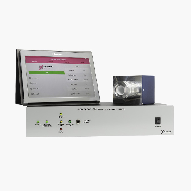
Evactron® E50 Plasma De-Contaminators™
Evactron® E50 淨化器是一款小巧高性能等離子清潔器,專為電子和離子束儀器(包括 SEM、TEM 和 FIB)而設計。 E50 提供強大的清潔功能,可增強解析度和成像,同時提高偵測器和探頭的靈敏度(污染可能會影響靈敏度)。 憑藉其高功率清潔功能,Evactron® E50 可確保在各種壓力下進行快速有效的清潔,從而獲得高品質、無偽影的影像並提高樣品分析效率。
VIEW MORE
-

Indium Phosphide (InP) Substrate
磷化銦 (InP) 基板。 III-V族化合物半導體材料由III族元素銦(In)和V族元素磷(P)結合而成。 應用特性:飽和電子漂移速度高、適合低損耗光纖通訊的發光波長、抗輻射能力強、導熱性能好、光電轉換效率高、禁帶寬度大。 應用範圍:廣泛應用於光模組元件、感測器元件、高階射頻元件等製造。
VIEW MORE
-
WSI-300晶圓AOI設備
VIEW MORE
-
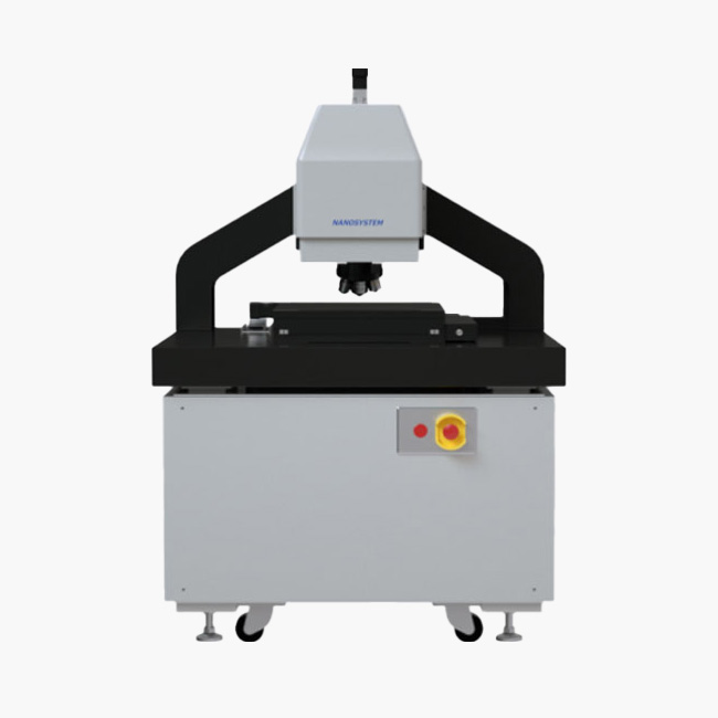
NV-F 2D/3D Hybrid Automation System - NV-F2700
最先進的非接觸式 3D 表面輪廓儀。
VIEW MORE
-
NV-F 2D/3D Hybrid Automation System - NV-F3200
最先進的非接觸式 3D 表面輪廓儀。
VIEW MORE


